Discrete Current Conveyor
What's a current conveyor?
Theory
Just as the opamp is a basic signal processing block for 'voltage mode' signal processing, the current conveyor is the equivalent for 'current mode'.
The CCII+ is a specific version of a current conveyor. It is a three terminal device (X,Y,Z) for which the relationship between the terminals can be defined in matrix form as,
From this relationship one sees that the current into Y is zero. The voltage applied to Y is seen at X, and the current that flows as a result from X is mirrored at the output Z. With some intuition, this can be related to a voltage follower circuit between Y and X, for which the output stage is part of a current mirror circuit to Z.
Why make a new one?
Current conveyors are not new and are well-understood in the literature. They are used in high speed signal processing designs due to higher achievable bandwidth with current mode processing.
At university, we were introduced to this device for analogue signal processing, but upon trying to buy myself one to play with (quick DigiKey search as is customary), I found that no such products were available.
PCB Design
Schematic
In order to accurately mirror the current from X to Z, the device requires good matching between the characteristics of the transistors on each side of the mirror. For a BJT design, this requires that the value and matching is good, such that two devices with the same will source approximately the same current through the collector. A similar logic is applied with matching MOSFETs.
In my work, I had stumbled across some interesting products from Nexperia, featuring matched BJTs in a single package such as the BCM847. These will provide sufficient matching for this prototype design. The schematic, captured in KiCad, for the discrete CCII+ is shown below.
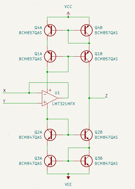
Features of note in this schematic include:
- The output drive to X is directly from the output stage of an opamp! The current consumption from the supply rails is mirrored.
- Wilson current mirrors have been used to provide the Z output.
Driving X direct from the LM7321 was a eureka moment, whilst playing in QSPICE with the design. Discrete implementation I had seen in my education implemented a push-pull stage outside the opamp, which was mirrored onto Z. The implementation seen here saves at least 2 devices by recognising that the push-pull stage is already implemented inside the opamp output stage and that the quiescent supply through U1 will flow through both mirrors and be cancelled at Z. Thinking this was very creative, I looked to see if anyone had in fact published this design and of course this exact circuit is shown in a figure from 40 years ago by a legend of the field (at least it means this isn't a silly approach),
Two new circuit approaches have been described, previously used for current convertors, to produce versatile precision CCII+ current conveyors suitable for monolithic fabrication. The performance of the discrete implementation offers a significant improvement over previous conveyor designs.
- HIGH-PERFORMANCE CURRENT CONVEYOR IMPLEMENTATION B. Wilson 17th October 1984
Whilst simulating the DC current error performance with single transistor current mirrors, poor behaviour was observed with varying output voltage. This was of course due to 'early effect' of the BJTs, or rather in analogue design terminology a finite output impedance of the mirror.
As seen above, the current through a BJT is not only dependent on the voltage, but also the voltage at the collector, which is undesirable for our CCII+ design as we wish the current out of Z to be independent of the voltage applied to the load on Z.
Implementing a four-transistor Wilson current mirror mitigates this problem by increasing the output impedance. With all engineering, no free lunch is had, and the additional transistor drops limit the output voltage swings achievable at X and Z, requiring larger supply voltages for the device. This design is really intended for something like +-12V rails in an audio signal processing design.
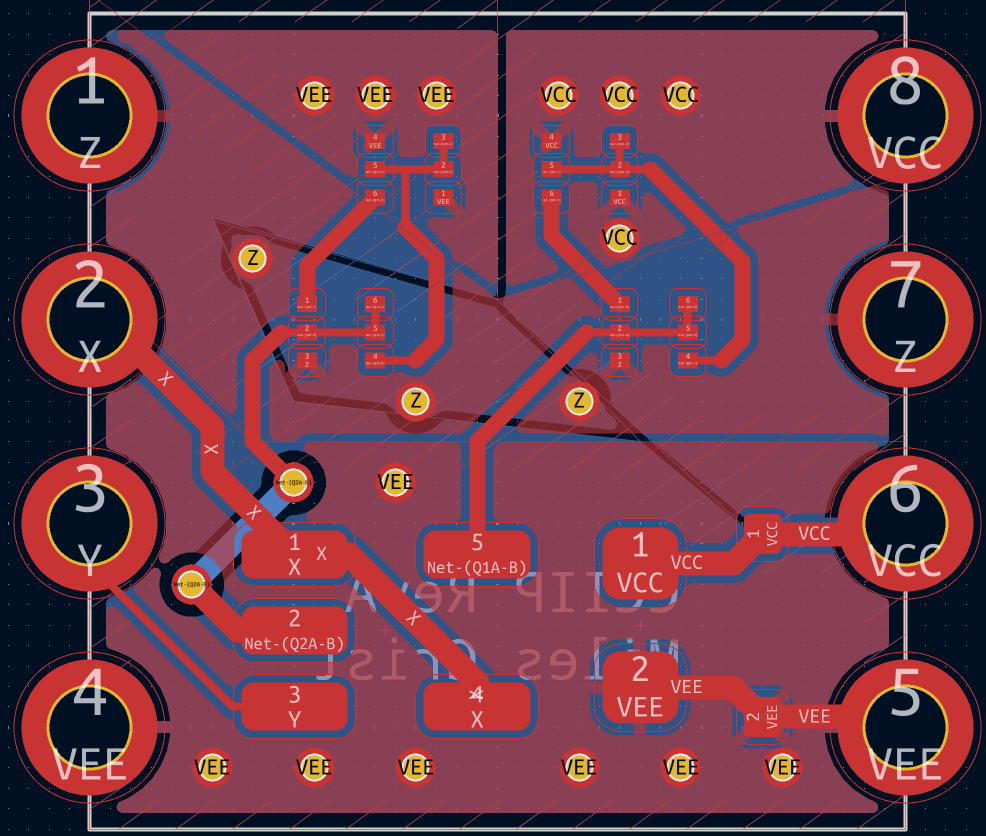
Layout
Wanting this design to be useful for low frequency (i.e. audio) analogue prototypes on a breadboard, the layout is designed with 0.1inch pin header in mind. To fit all the devices onto a tiny little board, the QFN package versions of the Nexperia BJTs were selected.
The Rev A was manufactured with JLCPCB in a 2-layer standard process, 0.8mm board thickness.
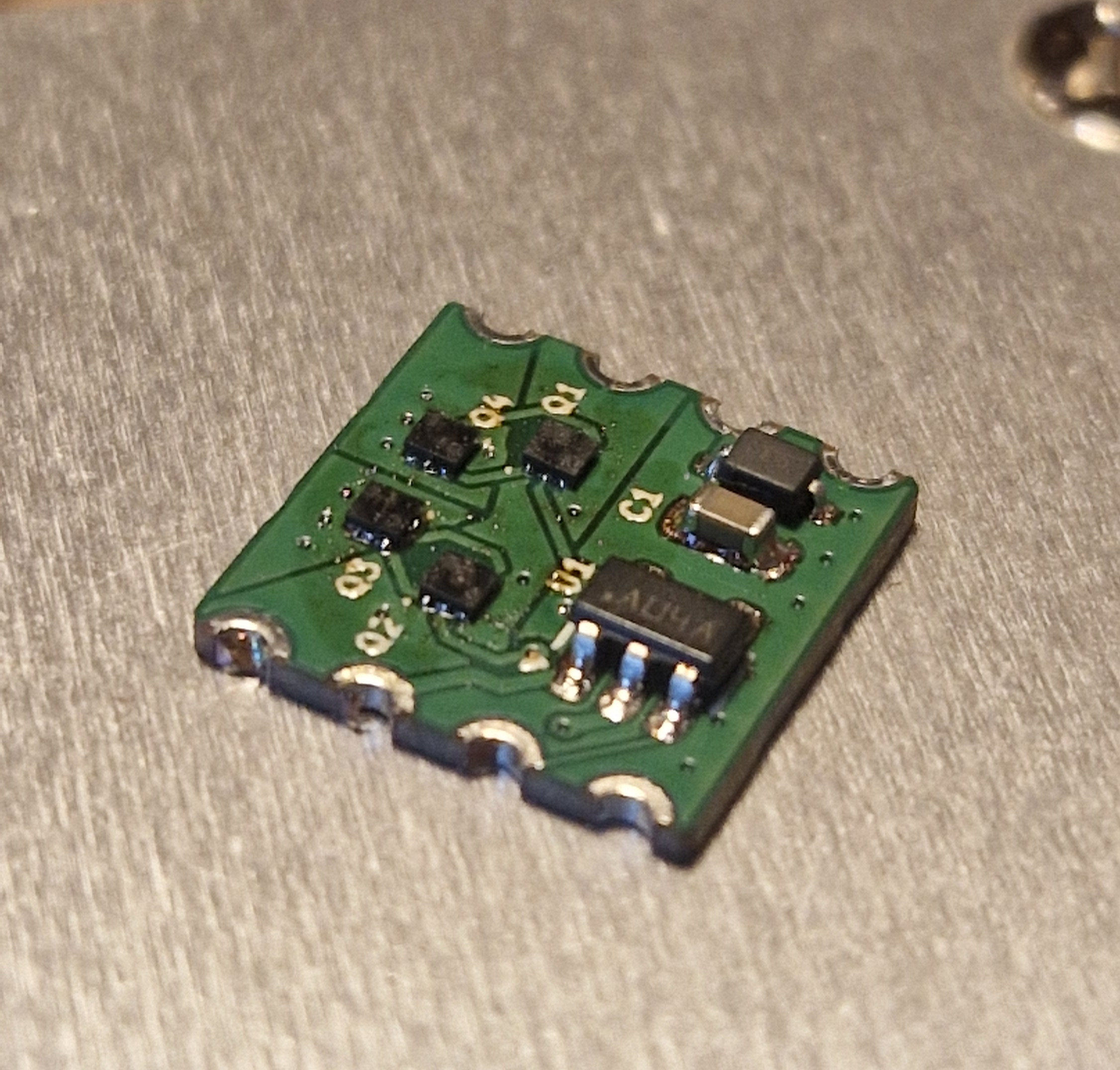
Hand Assembly
With a steel stencil produced by JLCPCB, I threw together a little jig and scraped some Chip Quik paste onto a board. Very quickly it became apparent that the apertures for the BJT pads were so small that paste was blocking holes or not adhering to the pads as the stencil was removed.
I dramatically overestimated my ability to solder the BJTs and began soaking boards with flux in desperation.
Regardless, 2 boards were laboriously produced on a USB PD hot plate.
Testing
WIP (smoke testing and basic behaviour done)